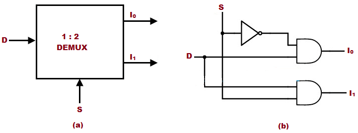
Logic Diagram For 2 Bit Demultiplexer
Demultiplexer Demux
Logicblocks Experiment Guide Learn Sparkfun Com

Demultiplexer Demux Digital Decoder Tutorial

Demux Demultiplexer Types Construction Applications

Binary Decoder Used To Decode A Binary Codes

Multiplexer Mux And Multiplexing Tutorial

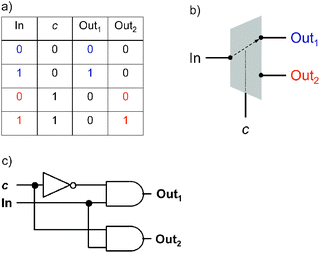
Or by expressing the circuit as shows that it could be two one bit 1 to 2 demultiplexers without changing its expected behavior.
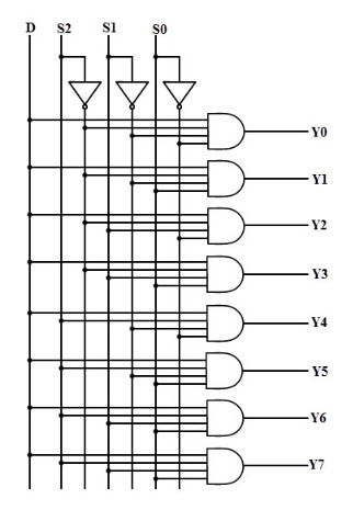
Logic diagram for 2 bit demultiplexer. Multiplier designing of 2 bit and 3 bit binary multiplier circuits. Multiplexer and demultiplexer the ultimate guide. Carry look ahead adder working circuit and truth table. The data inputs of upper 8x1 multiplexer are i 15 to i 8 and the data inputs of lower 8x1 multiplexer are i 7 to i 0.
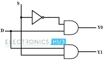
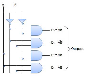
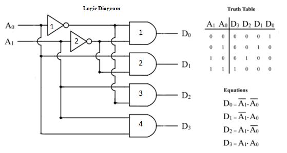
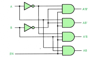
From the above truth table the logic diagram of this demultiplexer can be designed by using two and gates and one not gate as shown in below figure. Alu arithmetic logic unit in an alu circuit the output of alu can be stored in multiple registers or storage units with the help of demultiplexer. As an example a device that passes one set of two signals among four signals is a two bit 1 to 2 demultiplexer. We can implement 16x1 multiplexer using lower order multiplexers easily by considering the above truth table.
The same selection lines s 2 s 1 s 0 are applied to both 8x1 multiplexers. Multiplier designing of 2 bit and 3 bit binary multiplier circuits. Comparator designing 1 bit 2 bit and 4 bit comparators using logic gates. 4 bit parallel adder and 4 bit parallel subtractor designing logic diagram.
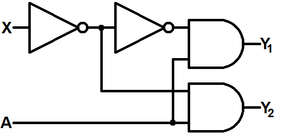
Looking for a logic diagram of a 2 bit demultiplexer i need a logic diagram of a 2 bit demultiplexer a circuit whose single input lie is steered t one of the four output lines depending on the state of the two control lines. When the select lines s 0 and gate a1 is enabled while a2 is disabled. The 2 to 4 line decoder demultiplexer like the multiplexer circuit the decoder demultiplexer is not limited to a single address line and therefore can have more than two outputs. The multiplexer and demultiplexer work together to carry out the process of transmission and reception of data in communication system.
Then the data from the input flows to the output line y1. Multiplexer and demultiplexer the ultimate guide. 1 to 4 demultiplexer the input bit is data d with two select lines a and b. The block diagram of 16x1 multiplexer is shown in the following figure.
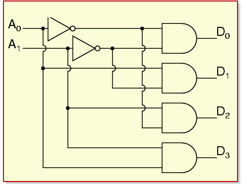
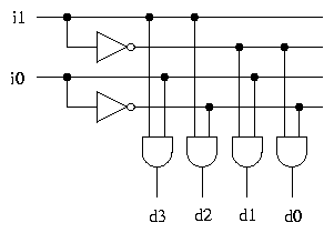
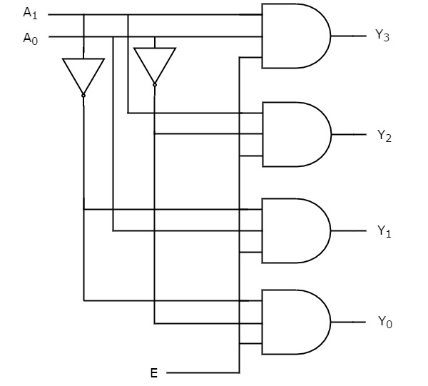
4 bit parallel adder and 4 bit parallel subtractor designing logic diagram. Comparator designing 1 bit 2 bit and 4 bit comparators using logic gates. Carry look ahead adder working circuit and truth table. A 1 to 4 demultiplexer can easily be built from 1 to 2 demultiplexers as follows.
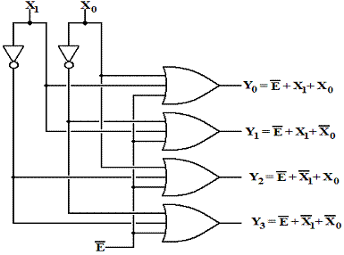
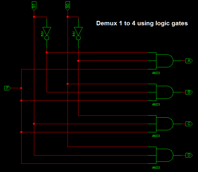
View forum posts. The 1 to 4 demultiplexer consists of one input four outputs and two control lines to make selections the below diagram shows the circuit of 1 to 4 demultiplexer.
How To Design Of 2 To 4 Line Decoder Circuit Truth Table And
Decoders And Multiplexers
Combinational Circuits Tutorialspoint
Demultiplexer Demux Types Cascading Applications And Advantages
Instrumentation In A Nutshell Decoder
Combinational Circuits Using Decoder Geeksforgeeks

9 6 Demultiplexers
More Combinational Circuits
Digital Circuits Decoders Tutorialspoint
Vhdl Code For 1 To 4 Demux

Comparator Designing 1 Bit 2 Bit And 4 Bit Comparators Using
A Molecular 1 2 Demultiplexer Chemical Communications Rsc

Binary Decoder Wikiwand